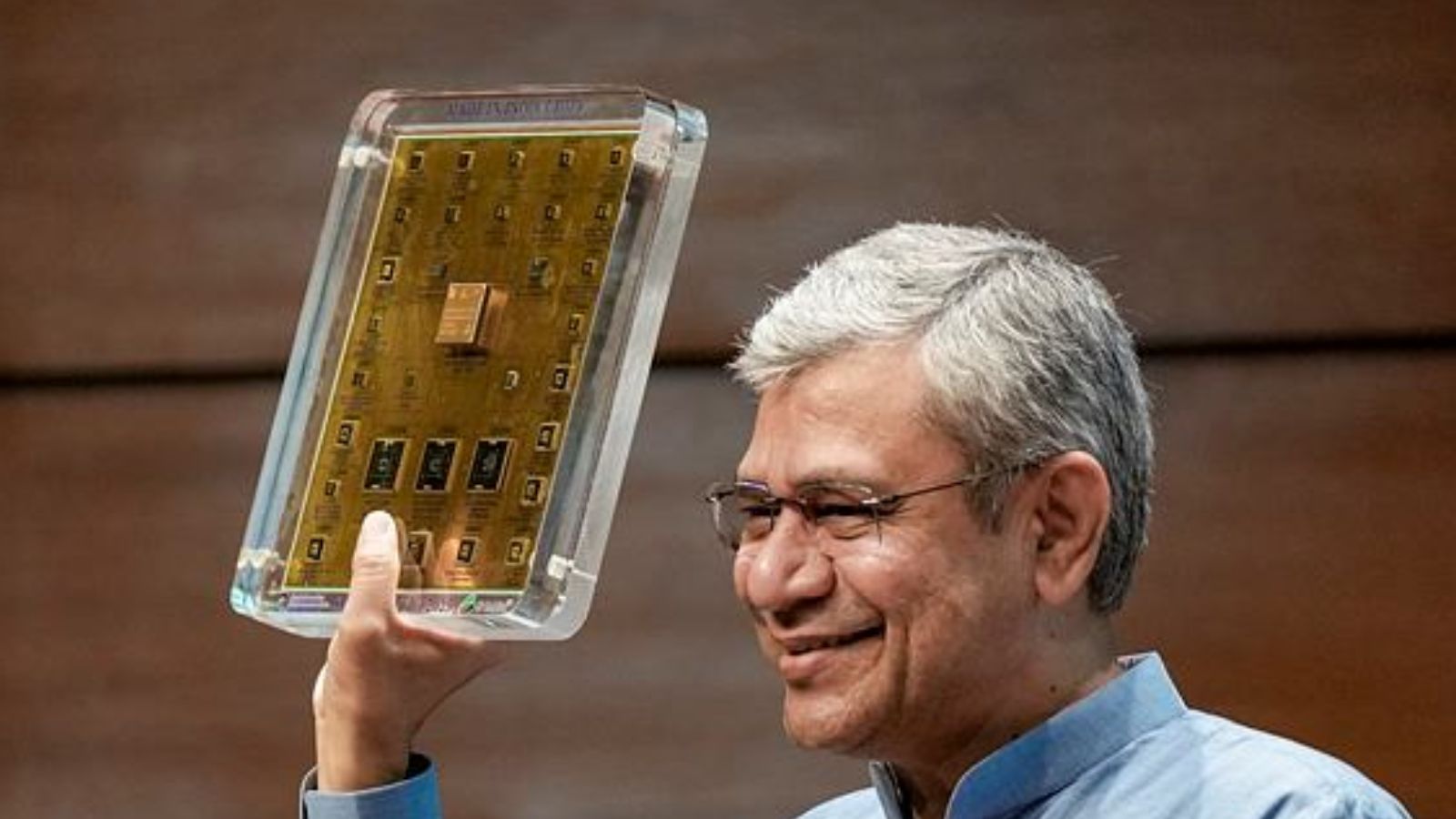
India Semiconductor Mission 2.0 marks a strategic pivot, removing subsidies for technology transfer and land acquisition to prioritize chip design and supply chain growth. With a revised outlay of Rs 1.27 lakh crore, the new scheme aims to bolster domestic capabilities and reduce reliance on opaque cost structures.
Key Takeaways
- No central subsidies for technology transfer or land acquisition; states must lead on land.
- Priority shifts to chip design, supply chain ecosystem, and R&D over manufacturing units.
- Capex subsidies for fabs reduced (50% to 40%/35%), with a new focus on the 7nm node.
The Government of India has recalibrated its ambitious semiconductor strategy with the launch of the India Semiconductor Mission (ISM) 2.0. In a significant move that underscores a maturing policy approach, the Centre has decided to discontinue subsidies for technology transfer costs and land acquisition for chip manufacturing plants. This decision stems from the realization that calculating technology transfer fees is often opaque and complex, making standardized disbursement difficult and prone to discrepancies.
Strategic Pivot: From Manufacturing to Ecosystem Growth
Under the previous iteration, the focus was heavily skewed toward attracting fabrication units (fabs). However, ISM 2.0 signals a paradigm shift. A senior government official revealed that the new hierarchy of priorities places chip designing at the forefront, followed by developing the broader supply chain ecosystem, and finally subsidizing the construction of new manufacturing units. This approach aims to create a holistic semiconductor environment rather than just isolated manufacturing islands.
Financial Implications and Incentive Structures
While the total financial outlay remains substantial at Rs 1.27 lakh crore, the deployment of funds has become more targeted. The uniform 50% capital expenditure subsidy for fabs seen in ISM 1.0 has been trimmed. Under the new scheme, silicon fabs will receive a 40% subsidy, while other fabs will get 35%. Incentives for advanced packaging have been set at 35%, and conventional packaging at 25%.
Crucially, the government is now open to taking equity in design startups and offering grants, contingent on private equity investment. Furthermore, the scheme offers robust support for ancillary industries—companies producing chip manufacturing equipment, chemicals, and gases can avail incentives of up to 30%.
Focus on Cutting-Edge R&D
Perhaps the most forward-looking aspect of ISM 2.0 is the heavy emphasis on Research and Development (R&D). The government is offering subsidies of up to 75% for R&D in cutting-edge chip design, specifically targeting the 7 nanometer node size. This is a strategic leap from the current commercial standard of 28nm, which is being targeted by players like Tata Electronics. By incentivizing advanced nodes, India aims to insert itself into the high-value segments of the global semiconductor supply chain, with a goal to meet 70-75% of domestic demand by 2029.